Smaller devices introducing new challenges
Semiconductor devices rely on wafers and thin films grown through repeated processes in a highly advanced computer chip machine. To enhance functionality and optimize wafer use, these devices are shrinking to the atomic scale thanks to novel materials and 3D designs. This shift increases the need for precise, non-destructive material inspection, especially as the industry adopts heterogeneous systems combining various semiconductors for better performance.
Current inspection methods of the wafers and thin films have limitations, such as surface-only analysis, destructive depth profiling, or insufficient accuracy in non-destructive approaches. These challenges hinder production quality, efficiency, and sustainability.
Focus of TeraTom project
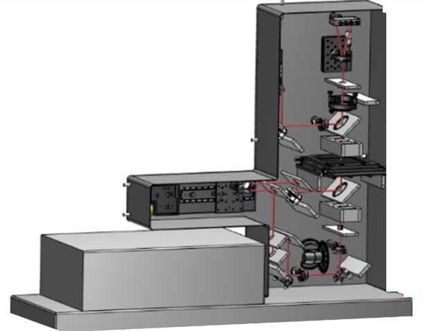
The granted TeraTom project aims to close this gap by exploring terahertz (THz) spectroscopy and microscopy techniques to analyze material properties across depth and position in heterogeneous and 2D systems. Researchers will develop a non-invasive, non-destructive prototype combining THz radiation and optical pulses for industrial applications. This tool will improve quality, yield, and efficiency while minimizing waste, bolstering the competitiveness of semiconductor manufacturers.
Consortium partners
TU/e, ARCNL, Saxion University of Applied Science, IMS, Aixtron, Applied Nanolayers, TeraNova, Smart Photonics, Bronkhorst High-Tech B.V., VSL. Supported by the Universiteitsfonds Eindhoven.