Metrology
Nanoscale Imaging and Metrology

About
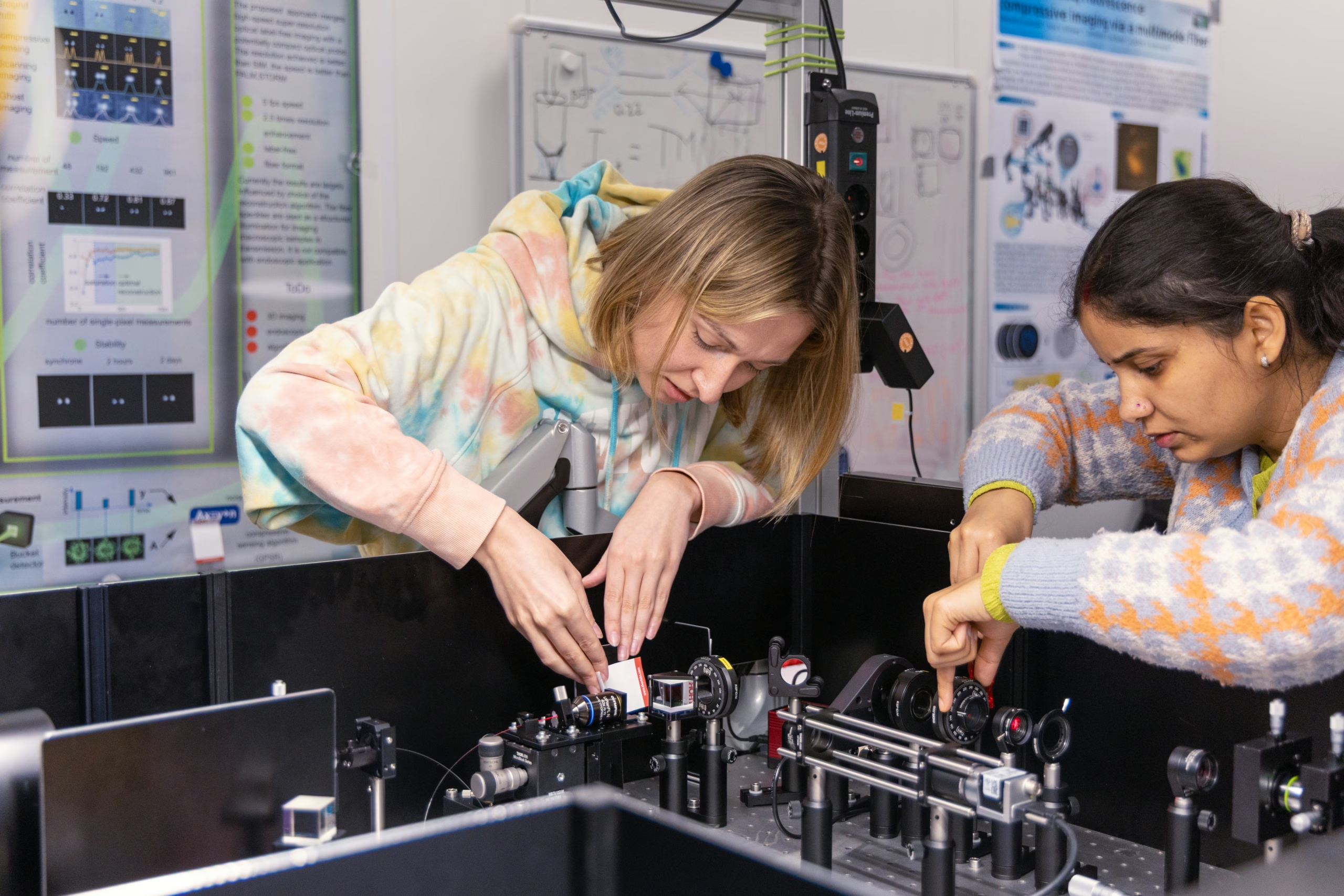
The Nanoscale Imaging & Metrology group develops advanced computational optical imaging and measurement tools that overcome limits of resolution and speed. Our goal is to enable fast, label-free imaging with extremely high spatial and temporal precision, supporting the growing needs of modern nanotechnology and semiconductor manufacturing.
Research focus
The group creates new imaging and metrology approaches for next-generation semiconductor and nanotechnology applications. Our research combines computational imaging, machine learning, compact fiber-based imaging and advanced optical microscopy, all aimed at enabling fast, high-resolution and three-dimensional inspection of tiny structures as electronic devices become smaller and more complex.
As electronic devices become smaller and more powerful, inspecting their tiny internal structures demands ever higher precision and extraction of useful data quickly. The Nanoscale Imaging & Metrology group uses machine learning, Bayesian optimization and computational imaging to push compact metrology tools beyond traditional limits.
The group also develops label-free optical imaging methods that surpass the diffraction limit and achieve higher temporal resolution, enabling them to visualize and characterize multilayer nanostructures. These methods combine compressive sensing with modern data-processing algorithms and are directly relevant to semiconductor device inspection.
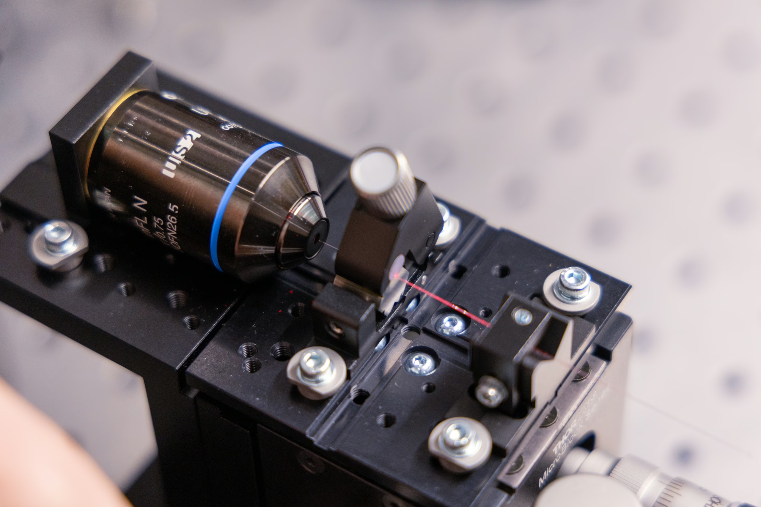
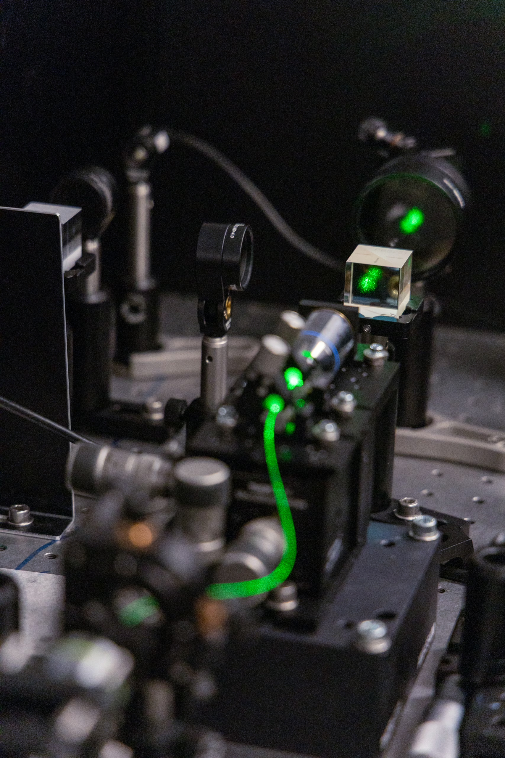
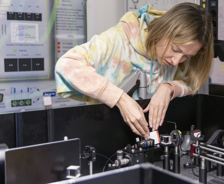
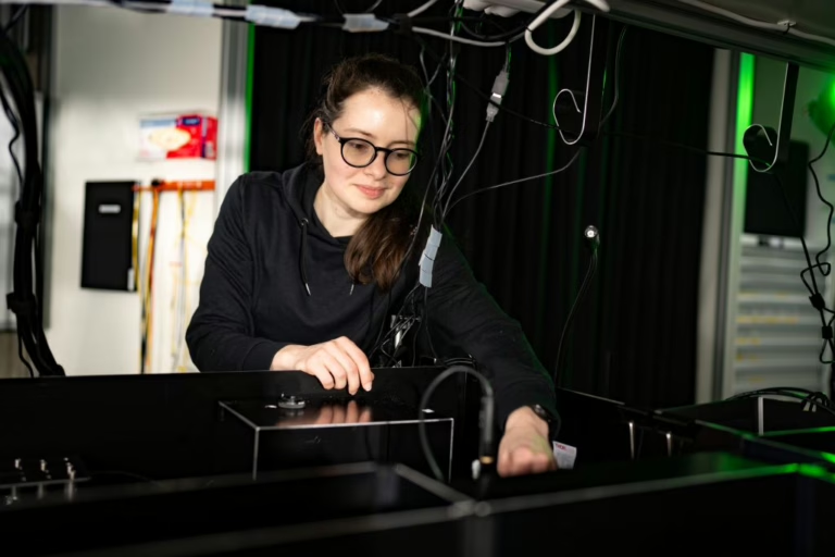
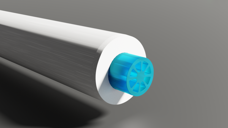
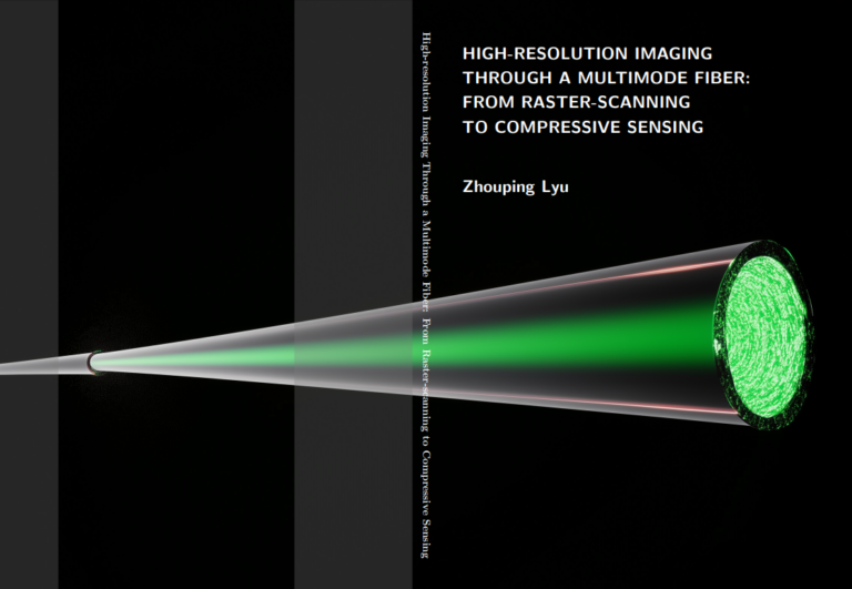
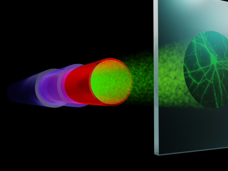
Optical fibers, particularly multicore or multimode varieties, offer a compact and flexible platform for imaging and wafer metrology. Researchers in the Nanoscale Imaging & Metrology group develop new methods of fiber-based imaging that enable precise characterization of nanoscale structures. Using spatial wavefront shaping, we control how light propagates through the fiber and the broader optical system, as well as how measured signals are formed. The fibers are further optimized to enhance light-collection (numerical aperture), flexibility and signal-to-noise ratio. On the computational side, we leverage compressive sensing: by exploiting sparsity together with engineered (randomly) structured illumination, we reconstruct high-quality images, exceeding conventional resolution limits.
The “coherence” of light – that is, the consistency of its wavefront and phase – plays a key role in accurate metrology, especially for semiconductor applications. We investigate how to engineer spatial coherence and wavefront properties using simple, cost-effective systems, for example through multimode fibers. Such control could significantly improve the precision and reliability of optical metrology tools used in lithography and chip manufacturing.
Our approach combines hardware developments (optical fibers and setups) with computational and signal-processing advances, aiming to deliver robust metrology solutions capable of meeting the demanding requirements of industry.
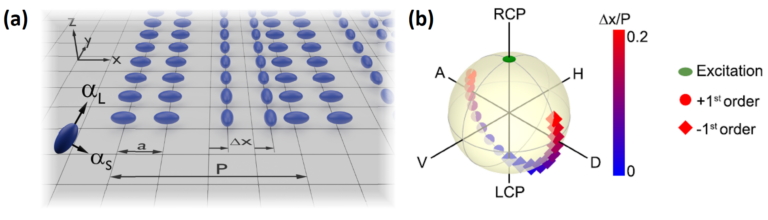
In one of our recent breakthroughs, we developed a method to measure sub-nanometer displacements between periodic nanostructures. Using specially designed metasurfaces and analyzing the full polarization state of diffracted light (instead of only its intensity), we achieve very high precision. This kind of metrology is crucial for aligning nanostructured layers in semiconductor manufacturing, where even tiny misalignments can affect device performance.
More generally, many of our imaging and metrology techniques are “label-free” (i.e., do not require fluorescent markers) and can work in far-field (no need for contact probes or lenses extremely close to the sample). This makes them well suited for industrial applications, such as high-throughput inspection in chip fabrication, as well as for more fundamental research.
Group members
Lyuba Amitonova leads the Nanoscale Imaging and Metrology group and holds an appointment as Associate Professor at VU Amsterdam. She combines expertise in optical metrology, computational imaging, and fiber-based imaging techniques, driving research aimed at practical and scalable solutions for nanolithography and semiconductor inspection.








Latest news




Most recent publications